
Glass substrate and TGV
Glass substrates are essential in advanced semiconductor packaging, including glass interposers with fine-pitch, high-aspect-ratio TGVs and glass cores with larger vias in thicker glass layers. Accurate inspection of these structures is critical to ensure product reliability. However, conventional tools often struggle to inspect internal features deeply buried inside the glass — especially tiny cracks or rough surfaces that may lead to failures. Holotomography captures the full 3D structure of vias and surrounding glass non-destructively. It can visualize internal features, sidewalls, subsurface cracks, and even provide cross-sectional images similar to observing a physical cut, without damaging the sample — regardless of via size, depth, or glass thickness (up to 2 mm).
A Through Glass Via (TGV) is a microscopic hole — typically tens of micrometers wide — formed through a glass substrate and later filled with metal so electrical signals can travel vertically through the glass. Glass is replacing organic materials in advanced chip packaging because it is flatter, more stable, and better at high frequencies. The catch: every via must be geometrically perfect, and the defects that kill reliability — subsurface microcracks, rough sidewalls, incomplete etching — are buried inside transparent glass, where surface inspection cannot see them and cutting the panel destroys it. That is exactly the gap holotomography fills.
Laser modification
A laser locally changes the glass structure where each via will form. HT checkpoint: image the modified zone and refractive-index change to verify laser parameters — before committing the whole panel to etching.
Selective etching
Chemical etching removes the modified glass, opening the via. HT checkpoint: measure top/bottom diameter, taper, depth, sidewall roughness, and detect residues or microcracks — without cross-sectioning.
Metallization
The via is filled with copper to become a working interconnect. HT checkpoint: confirm via geometry and integrity pre-fill, so plating defects are prevented rather than discovered at electrical test.
Features
-

- Full 3D Via Imaging
- Capture the entire 3D structure of vias, including depth, sidewalls, and bottom.
-

- Crack Detection
- Detect internal micro-cracks inside the glass.
-
- Wide Aspect-Ratio Range
- Measures narrow/deep and wide/shallow vias across a broad AR range.
-
- Deep Glass Inspection
- Non-destructive 3D imaging up to 2 mm glass thickness.
Discover Glass substrate and TGV with HT
-
Laser Modification Analysis
Holotomography non-destructively maps laser-induced RI changes and micro-cracks inside glass for optimized TGV formation.
• Visualizes laser-modified regions inside glass in high-resolution 3D
• Quantifies minute refractive index changes caused by laser processing
• Detects and characterizes internal micro-cracks before selective etching
• Supports optimization of laser parameters for stable TGV formation
• Replaces destructive cross-section analysis with rapid, spatial 3D data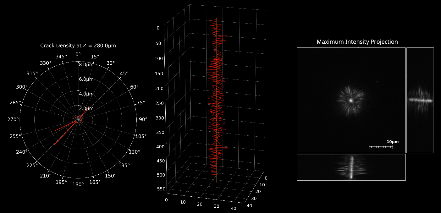
3D crack-density mapping and MIP (Maximum Intensity Projection) analysis of laser-modified glass
-
Optimized Etching Process Control
Holotomography enables fast, non-destructive 3D analysis of etched TGV structures to optimize via geometry, sidewall quality, and process stability.
• Measures CD (Critical Dimension), taper angle, and full 3D internal profile
• Verifies structural uniformity across glass-core substrates
• Detects etching residues, sidewall roughness variations, and micro-defects
• Reduces reliance on destructive cross-sectioning for process validation
• Supports rapid calibration of etchant concentration and etching time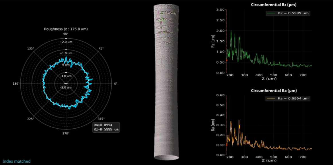
Non-Destructive 3D Mapping of Etched TGV Geometry and Inner-Wall Roughness
-
Enhanced AOI Inspection Support
Holotomography adds high-resolution 3D validation to AOI defect candidates, reducing false calls and overkill.
• Provides 3D confirmation of defect candidates
• Classifies voids, micro-cracks, and internal defects with sub-micron spatial data
• Reduces false calls/overkill by distinguishing real defects from AOI artifacts
• Replaces destructive cross-sectioning with non-destructive defect validation
• Supports root cause analysis and process optimization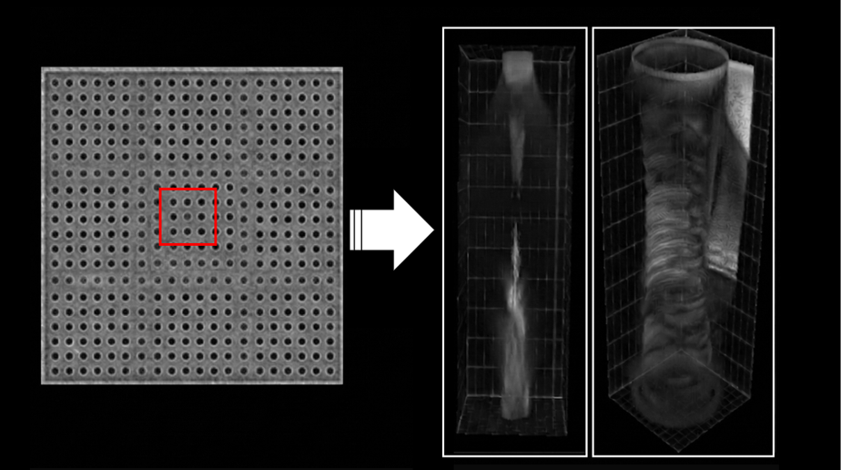
High-Resolution 3D Verification of AOI-Detected TGV Defects
What You Can Measure
Every claim above, translated into the concrete numbers a process engineer takes away from one non-destructive scan.
| Via geometry | Top / bottom diameter, depth, taper angle — full 3D profile of every via in the field, across a wide aspect-ratio range |
|---|---|
| Sidewall roughness | 3D sidewall profile over the entire inner wall — not a single line scan at a cut plane |
| Internal microcracks | Location and extent of subsurface cracks around vias, before they become field failures |
| Laser-modified zone | 3D refractive-index map of the modification volume (sensitivity ~10⁻⁴ Δn) for laser parameter tuning |
| Etch completeness | Residue detection and profile uniformity across the panel, up to 2 mm glass thickness |
| Virtual cross-sections | Cross-sectional images analogous to a physical cut, obtained non-destructively — with zero panels sacrificed |
* Application notes with measured datasets are available on request.
Send us your TGV sample
Evaluating holotomography for TGV process control? The fastest path is your own panel.
We measure it free of charge and review the full 3D dataset with you.
- 01Send your sample
under NDA - 02We measure it and prepare
a full 3D analysis report - 03Review the data live
with our application engineer